VG-4511CA 153.6000M-GGCT3 数据手册
Crystal oscillator
Epson Toyocom
Product Number (please contact us)
X1G002781xxxx00
VOLTAGE -CONTROLLED CRYSTAL OSCILLATOR (VCXO)
VG - 4511CA
•Frequency range
•Supply voltage
•Absolute pull range
•External dimensions
•Function
:
:
:
:
:
80 MHz to 170 MHz LV-PECL
3.3 V
-6
±50 × 10
7.0 × 5.0 × 1.6 t (mm) Typ.
Output enable(OE)
Actual size
Specifications (characteristics)
Item
Symbol
Specifications
fO
Output frequency range
Remarks
Please contact us for inquiries regarding
available frequencies.
80.000 MHz to 170.000 MHz
Supply voltage
VCC
3.3 V ±0.165 V
Storage temperature range
T_stg
-55 °C to +125 °C
Operating temperature range
T_use
As per below table.
-6
Frequency tolerance
f_tol
±50 × 10 Max.
Current consumption
ICC
70 mA Max.
-6
Absolute pull range
APR
GCT:±50 × 10 Min.
Input resistance
Rin
100 kΩ Min.
Frequency change polarity
Positive slope
Symmetry
SYM
40 % to 60 %
High output voltage
VOH
Vcc-1.1 V Min.
Low output voltage
VOL
Vcc-1.5 V Max.
Output load condition (ECL)
L_ECL
LV-PECL
VIH
70 % VCC Min.
Output enable / disable input
voltage
VIL
30 % VCC Max.
Rise time / Fall time
tr / tf
1.5 ns Max.
Start-up time
t_str
10 ms Max.
Frequency aging
f_aging
This is included frequency tolerance
* Please keep VC pin open or ground while powering up VCC.
Store as bare product after unpacking
Includes frequency aging (20 years)
No load condition.
VC= 1.65 V ± 1.5 V
DC level
VC= 0 to 3.3 V
–
–
–
VIH or OPEN : Enable
VIL or GND : Disable
20 % VCC to 80 % VCC level
Time at minimum supply voltage to be 0 s
+25 °C, VCC=3.3 V, 20 years
Operating temperature range
Operating temperature range
40 °C~+85 °C
20 °C~+70 °C
0 °C~+70 °C
GGCT
JGCT
KGCT
External dimensions
Footprint (Recommended)
(Unit :mm)
(Unit :mm)
7.0±0.2
#4
#5
1.8
E 155.520
C=0.1 µF Min.
#5
#6
#4
VAG674A
#1
2.0
5.0±0.2
#6
C
#3
1.4
4.2
1.6±0.2
#2
1.2
Pin map
2.6
C0.5
2.54
2.54
Pin
1
2
3
4
5
6
Resist
Cconnection
Vc
OE
GND
OUT1(Positive)
OUT2(Negative)
Vcc
Note.
OE Pin
OE pin = "H" or "open" : Specified frequency output.
OE pin = "L" : Output is high impedance, oscillation stops.
http://www.epsontoyocom.co.jp
#1
#2
#3
5.08
To maintain stable operation, provide by-pass capacitor with
more than 0.1 μF at a location as near as possible to the power
source terminal of the crystal products (between VCC - GND).
�
VG-4511CA 153.6000M-GGCT3 价格&库存
很抱歉,暂时无法提供与“VG-4511CA 153.6000M-GGCT3”相匹配的价格&库存,您可以联系我们找货
免费人工找货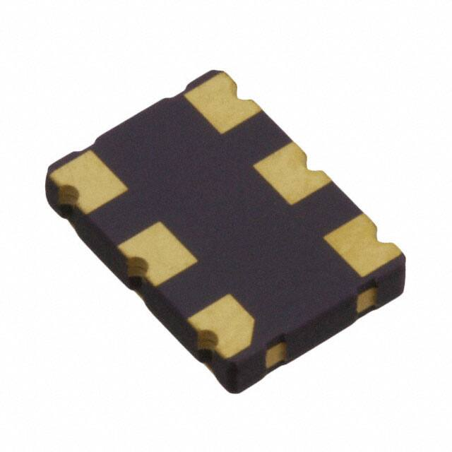


 工商网监
湘ICP备2023018690号
工商网监
湘ICP备2023018690号
